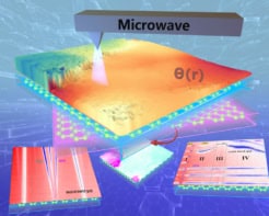
Using a technique known as strain engineering, researchers in the US and Germany have constructed an “excitonic wire” – a one-dimensional channel through which electron-hole pairs (excitons) can flow in a two-dimensional semiconductor like water through a pipe. The work could aid the development of a new generation of transistor-like devices.
In the study, a team led by Vinod Menon at the City College of New York (CCNY) Center for Discovery and Innovation and Alexey Chernikov at the Dresden University of Technology and the University of Regensburg in Germany deposited atomically thin 2D crystals of tungsten diselenide (fully encapsulated in another 2D material, hexagonal boride nitride) atop a 100 nm-thin nanowire. The presence of the nanowire created a small, elongated dent in the tungsten diselenide by slightly pulling apart the atoms in the 2D material and so inducing strain in it. According to the study’s lead authors, Florian Dimberger and Jonas Ziegler, this dent behaves for excitons much like a pipe does for water. Once trapped inside, they explain, the excitons are bound to move along the pipe.
Highly anisotropic exciton motion
To monitor the motion of the excitons, the researchers used a combination of techniques. In the first, known as transient microscopy, they used pulses of light to excite the hybrid 1D/2D structure and thus reveal the excitons’ location. The second technique, time-resolved luminescence, involved imaging the electron-hole pairs with a streak camera. In this way, they could observe exciton transport at both cryogenic temperatures and room temperature.
Their results showed that the excitons’ movement is highly anisotropic, occurring only along the direction of the channel. Indeed, the researchers determined the coefficient of exciton diffusion along the nanowire direction to be as high as 13.5 ± 1 cm2/s, corresponding to an effective exciton mobility at room temperature of 540 cm2/Vs. In contrast, exciton diffusion in the perpendicular direction, across the channel, dropped almost to zero.
Controlling excitons in other low-dimensional structures
The tungsten diselenide material used in this experiment is part of a family known as transition metal dichalcogenides (TMDCs). These layered van der Waals (vdW) materials have the chemical formula MX2, where M is a transition metal such as molybdenum or tungsten and X is a chalcogen such as sulphur, selenium or tellurium.
In their bulk form, TMDCs act as indirect band-gap semiconductors. When scaled down to monolayer thicknesses, however, they are direct band-gap semiconductors capable of absorbing and emitting light very efficiently. This property makes 2D TMDCs highly attractive building blocks for devices such as light-emitting diodes, lasers, photodetectors and solar cells. They could also be used to make circuits for low-power electronics and sensors. What is more, unlike bulk semiconductors, which are usually brittle, TMDCs can withstand in-plane strain as high as 11%, making them promising materials for flexible electronic devices and sensors for mechanical deformations.
Excitons in TMDCs are straightforward to create by exciting the material with light. They are also tightly bound and extremely stable, and unlike electrons they do not carry a charge. Being able to manipulate their movement is therefore an important step towards making devices from electrically neutral quasiparticles. Such devices could work at room temperature and might replace certain tasks performed by current transistor technology in a merger of optics and electronics, the researchers say.

Strain induces nonlinear Hall effect in monolayer material
The new platform, which is detailed in Science Advances, might also be used to control excitons in a wide range of other low-dimensional structures, they add. These include vdW heterostructures designed to host so-called Moiré-like excitations.
Truly 1D exciton motion
While their present work describes quasi-1D transport of excitons with near 100% anisotropy, the researchers suggest that the same approach could also be scaled down to obtain channel widths on the order of just tens of nanometres. Such narrow channels are expected to exhibit truly 1D exciton motion and could reveal quantum transport phenomena, such as Luttinger liquid behaviour or many-body localization effects.
Looking ahead, the team says it now plans to explore the ability of these excitonic channels to carry spin information. “This knowledge will be an important step for future circuits based on excitons instead of electrons,” Menon tells Physics World.