An international team of researchers has succeeded in steering light waves deep into “forbidden” regions of photonic crystals by manipulating the shape of the waves. The technique, which was developed by scientists at the University of Twente in the Netherlands, the University of Iowa, US and the University of Copenhagen, Denmark, takes advantage of nanoscale channels created naturally when the crystals are fabricated, and could find use in a host of optoelectronics applications.
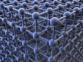
Photonic crystals are made by etching patterned nanopores into a substrate such as a silicon wafer. These patterned structures are specially designed to make the crystal’s refractive index vary periodically on the length scale of visible light. This periodic variation, in turn, produces a photonic “band gap” that affects how photons propagate through the crystal – similar to the way a periodic potential in semiconductors affects the flow of electrons by defining allowed and forbidden energy bands.
The presence of this band gap means that only light within certain wavelength ranges can pass through the crystal. Outside these ranges, the light is reflected due to an effect called Bragg interference. The prohibition on light travel at forbidden wavelengths is so restrictive that if a quantum dot that emits light at one of these wavelengths is placed inside the crystal, it stops emitting the forbidden colour of light.
“Out of control”
Photonic crystals were discovered 30 years ago, and they are now routinely integrated into devices such as light sources, lasers, efficient solar cells and so-called invisibility cloaks. They are also used to trap light in extremely small volumes and to process optical information. In addition, the ability to tightly control their emission properties makes them attractive for advanced applications such as nonlinear processors for quantum computing and memories that store information encoded as light.
To date, all these applications have been static, because the structure of the crystals (and thus the path of the light transported within them) is fixed. New functionalities should be possible, however, if light can be controllably steered anywhere inside the crystals, beyond the depth set by Bragg interference.
“This depth is known as the Bragg length and is determined by the intentionally introduced periodic structural order in the crystal when it is fabricated,” explains study lead author Ravitej Uppu. “Disorder arising from unavoidable imperfections in the nanofabrication process, however, produces channels that penetrate deep into the crystal and through which the trajectory of incoming light waves can be deviated. These channels are usually detrimental for applications because they allow a small fraction of waves to ‘get out of control’ and randomly scatter into the crystal.”
Light-steering demonstration
Led by Willem Vos of the University of Twente, Uppu and colleagues have now turned these channels and the fact that light waves can travel through them into an advantage. They did this by shaping the wavefronts of light waves so that they selectively couple to these channels, thus allowing the waves to travel much further into the crystal. What is more, by programming the wavefronts correctly, they could interfere the waves such that their intensity concentrates at a single location deep inside the crystals.
In their work, published in Physical Review Letters, the researchers studied light propagation in two-dimensional photonic crystals consisting of large periodic arrays of pores (about 6 microns deep) etched in a silicon wafer. They began by directing unstructured, random, plane light waves onto the crystals and imaging the light that leaks through the structures’ top surface. This leaked light revealed the energy density of light at any given position inside the crystals, and as the researchers expected, they saw hardly any sign that light had penetrated the crystal at all. They confirmed this result by showing that 95% of the incident light was reflected.
Eight times the Bragg length
The researchers then repeated their experiment using light waves with wavefronts shaped using a device known as a spatial light modulator. By programming the shapes, they managed to steer the waves into otherwise forbidden gaps in the crystal, travelling up to eight times the Bragg length. Focusing this light allowed them to create a bright spot that is up to 100 times more intense compared to that created by unshaped wavefronts.
My favourite Nobel prize: X-ray diffraction to deduce crystal structure
Members of the team say they now plan to extend their experiments to 3D photonic band gap crystals, where they “eagerly expect” to see additional phenomena such as Anderson localization of light. “Such 3D control of light transport could be exploited for exotic light hopping across a lattice of cavities inside these crystals,” Uppu tells Physics World. “The combination of reconfigurable light transport and cavities could potentially allow us to realize nonlinear quantum operations for quantum computing.”
And that is not all. Since the observed phenomena are essentially exploiting wave interference, the team is confident that their results can be generalized to electron waves, magnetic spin waves or even sound waves. Indeed, Uppu notes that other researchers have recently made considerable advances in the latter two fields, so the required spatial shaping of these waves should be feasible.