Available to watch now, HORIBA Scientific explores recent advances in nanoscale Raman characterization of new 2D materials and heterostructures
Want to learn more on this subject?
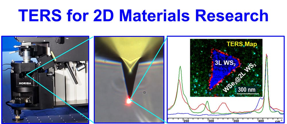
From graphene to TMDCs and beyond, Raman spectroscopy and Raman imaging proved to be extremely useful for characterization of 2D materials and visualization of various heterogeneities that occur naturally or are created on purpose. Quite often the scale of structural, electronic or morphological heterogeneity in these materials is on the order of a few tens of nanometres or less, which is beyond the spatial resolution of conventional Raman microscopy. Tip enhanced Raman scattering (TERS) and tip enhanced photoluminescence (TEPL) can address the problem of spatial resolution.
In this webinar we’ll demonstrate how TERS can enable Raman imaging of MXenes, a new class of 2D materials; probe number of nanoscale heterogeneities in 2D crystals: growth related, including lateral and vertical heterostructures, substrate induced, and the morphological heterogeneities that appear (intentionally or not) in the process of exfoliation/2D crystal transfer. Finally, we’ll discuss recent results on TERS imaging of reconstructed Moiré patterns in twisted bilayers of graphene.
Want to learn more on this subject?
Andrey Krayev is the US AFM-Raman Product Manager at HORIBA Scientific. Andrey Krayev received his master’s degree from the Moscow Institute of Physics and Technology, in 1991. In 2001, he started to use SPM, while working as an application scientist for QPT, Inc. Since 2008, he was the CTO at AIST-NT, Inc. and was actively involved in the development of the TERS technique and its implementation for real-world applications. Since the acquisition of AIST-NT technology by HORIBA in July of 2017, Andrey has held the position of the US AFM-Raman manager at HORIBA. He continues active development of TERS-related applications for advanced characterization of 2D materials and beyond.