The Fall Meeting of the Material Research Society will welcome delegates back to Boston, Massachusetts, while also delivering a virtual event to reach the global scientific community

This year’s Fall Meeting of the Materials Research Society will, like many other scientific conferences at the moment, be held as a hybrid event. Delegates can choose between attending the live conference in Boston, Massachusetts, or catching up with all the symposia and featured events through a dedicated virtual meeting.
The live conference will take place from 29 November through to 2 December, and with networking and social events will enable attendees to reconnect with friends and colleagues who they may not have seen for some time. The virtual meeting will follow a few days later, on 6–8 December, allowing registrants to access all the symposia and presentations on demand. Registrants for the virtual meeting will also be able to tune into a live stream of featured talks during the live event.
Whether attending in person or online, the MRS Fall meeting will provide a forum for discussing breakthrough materials research. The Symposium X sessions, which are designed to highlight work at the frontiers of materials science, will include talks on superconducting qubits for quantum computers, the internal structure of biominerals, and novel materials for next-generation lithium-ion batteries.
The scientific programme will also feature two Nobel laureates: Sir Kostya Novoselov of the University of Manchester in the UK will deliver the distinguished keynote lecture on Wednesday 8 December, while in the plenary session on Tuesday 9 December Sir Fraser Stoddart of Northwestern University in the US will highlight recent advances in artificial molecular machines.
Registrants to both the live and virtual meetings also have the opportunity to engage with scientific equipment vendors, either in the exhibit hall at the Hynes Convention Center or via online exhibit booths. Some of the latest innovations that will be presented are highlighted below.
Single instrument combines synchronous source and measure capabilities
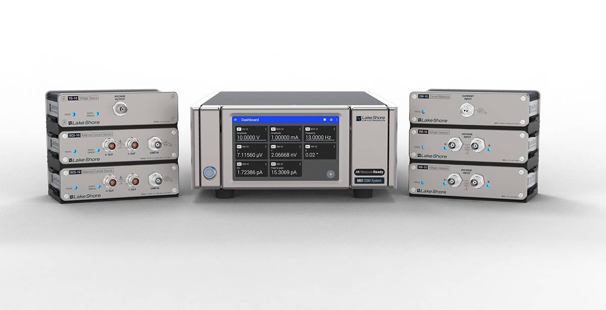
The new, modular M81-SSM (Synchronous Source and Measure) System from Lake Shore Cryotronics provides a flexible and powerful solution for a wide range of material characterization applications. The M81-SMM combines highly synchronized DC, 100 kHz AC, and mixed DC + AC sourcing and measuring in a single instrument, and also offers both voltage and current lock-in measurement capabilities.
The multichannel system supports up to three remote mountable source and three measurement modules, while its unique modular architecture enables signal and source amplifiers to be located as close as possible to the sample being characterized. Minimizing the signal wiring to the sample reduces noise and increases sensitivity, resulting in more accurate and repeatable measurements.
The amplifier modules feature 100% linear circuitry and leverage the M81’s patent-pending MeasureSync™ real-time sampling technology, which ensures synchronous sourcing and measuring across all channels. Multiple samples can be characterized under simultaneous sampling conditions to enable users to obtain consistent data. Combining both DC and AC sourcing and measurement in a single instrument reduces the need for different pieces of equipment, simplifying the set-up and operation of complex characterization configurations.
The M81-SSM system also uses the standard SCPI programming interface and is supported by Lake Shore’s MeasureLINK™ application software, which provides easy control of temperature and field set-up. The software also supports general electrical characterization measurements, with enhanced versions available for custom applications.
- Visit Lake Shore Cryotronics at booth #417
Automated imaging speeds up AFM experiments
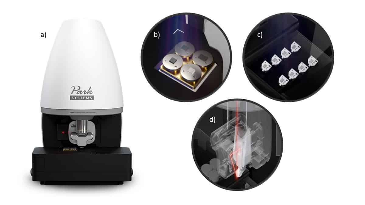
The latest atomic force microscope from Park Systems, the Park FX40, integrates robotics and machine learning throughout the design to produce the first AFM that fully automates the imaging process for research users. The FX40 exploits a robotic system to automatically change and replace its own tips, and also features an optical design that enables automatic beam alignment.
“The Park FX40 takes care of all the set up before and during scanning,” says Ryan Yoo, the company’s vice president for product development. “All the tedious and time-consuming manual processes are now a thing of the past. The Park FX40 performs them all autonomously.”
The FX40 also features a unique dual-camera design that makes it much simpler to locate the region of interest. The first camera offers a view of the whole sample stage, which can accommodate up to four samples at a time, to allow the user to quickly find and select the target location. The stage then automatically moves to the chosen position, at which point the system switches to a high-resolution camera for a closer view and any detailed adjustment.
Once in the correct location, the system automatically brings the probe close enough to the sample’s surface for measurements to be taken. With the FX40, Park Systems has also updated its true non-contact mode to boost the data quality and the precision of measurements.
- Visit Park Systems at booth #613
Materials support TEM nanocharacterization

MilliporeSigma supplies a variety of specialized materials for characterizing nanomaterials and nanodevices using transmission electron microscopy (TEM). The most detailed information can be obtained from TEM studies when the samples for analysis are mounted onto a TEM grid that matches the type of material to be studied.
TEM grids are available from MilliporeSigma in different materials, including copper, nickel and molybdenum, as well as with a range of mesh patterns and sizes. Grids are also available with a choice of films for supporting the specimen, such as a continuous amorphous carbon film with various thicknesses or a lacy carbon film with different hole sizes.
Locator and finder grids, which are used to quickly and easily check a particular feature, or to examine another TEM, are also available in a variety of designs and materials. In addition, MilliporeSigma offers a comprehensive range of supporting components for characterizing nanomaterials, including tweezers, TEM window grids with various thicknesses, a magnetic pick-up tool, cryo-capsules, and lift-out grids in copper and molybdenum. Substrates for atomic force microscopy are also available in various dimensions.
Breakthrough analyser delivers precision ARPES measurements for small samples
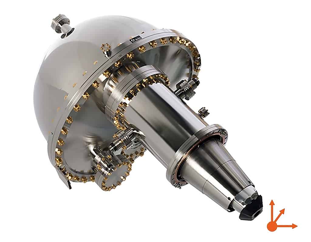
New from Scienta Omicron is the DFS30, a next-generation analyser for angular-resolved photoemission spectroscopy (ARPES). The DFS30 – which is now available as part of the company’s ARPES Lab system – is optimized for measuring the small-spot band structure of novel materials and micron-sized samples, and is perfect for measuring the electronic band structure of 2D materials.
High-quality ARPES measurements, particularly on small samples, require accurate alignment of the photon source, the sample, and the focal point of the analyser. The DFS30 exploits electrostatics to adjust the focal point of the analyser, for the first time replacing imprecise mechanical movements. This speeds up the workflow and improves reproducibility when optimizing experimental conditions.
The DFS30 extends Scienta Omicron’s wide range of analytical and turnkey solutions for surface science and nanotechnology. The company’s field-proven technologies provide configurable solutions for both standalone systems and for full Materials Innovation Platforms (MIPs) that offer full control over the materials development process.
One of these MIPs might include an epitaxial growth system for creating a material structure, an XPS Lab to evaluate the sample’s surface composition, or a bulk-sensitive 9.25 kV HAXPES Lab to probe interfaces below the surface. Other options include the HiPP Lab for studying gas or liquid surface interfaces under ambient pressure using XPS, and the LT STM for studying surfaces at ultralow temperatures with STM, spectroscopy, and Scienta Omicron’s QPlus® AFM.
- Visit Scienta Omicron at booth #318